- 您现在的位置:买卖IC网 > Sheet目录2002 > ISL83075EIBZA (Intersil)IC TXRX RS485/422 3.3V ESD 8SOIC
15
All Intersil U.S. products are manufactured, assembled and tested utilizing ISO9000 quality systems.
Intersil Corporation’s quality certifications can be viewed at www.intersil.com/design/quality
Intersil products are sold by description only. Intersil Corporation reserves the right to make changes in circuit design, software and/or specifications at any time without
notice. Accordingly, the reader is cautioned to verify that data sheets are current before placing orders. Information furnished by Intersil is believed to be accurate and
reliable. However, no responsibility is assumed by Intersil or its subsidiaries for its use; nor for any infringements of patents or other rights of third parties which may result
from its use. No license is granted by implication or otherwise under any patent or patent rights of Intersil or its subsidiaries.
For information regarding Intersil Corporation and its products, see www.intersil.com
FN6115.5
October 5, 2012
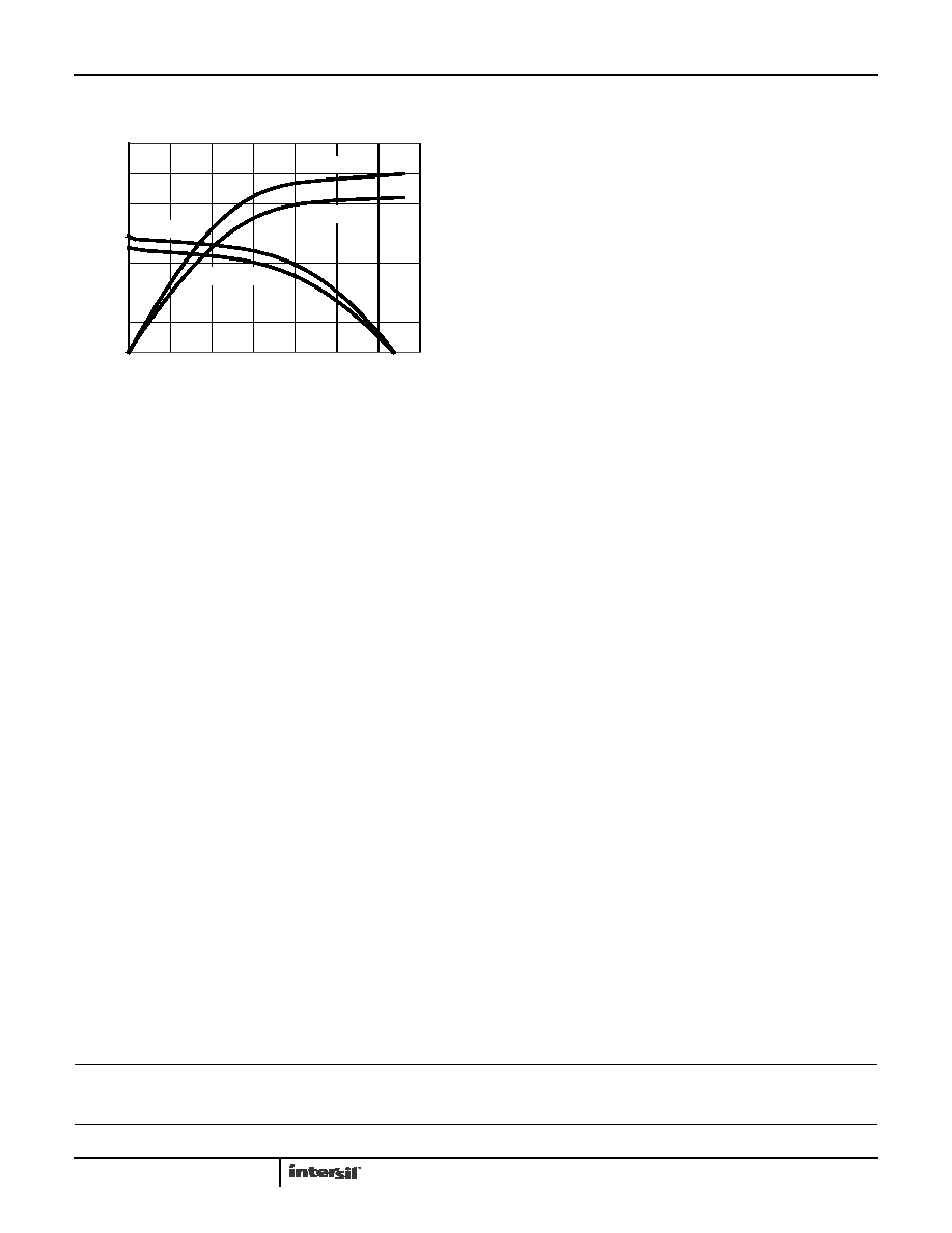
FIGURE 23. RECEIVER OUTPUT CURRENT vs RECEIVER
OUTPUT VOLTAGE
Die Characteristics
SUBSTRATE POTENTIAL (POWERED UP):
GND
TRANSISTOR COUNT:
535
PROCESS:
Si Gate BiCMOS
Typical Performance Curves VCC = 3.3V, TA = +25°C; Unless Otherwise Specified (Continued)
RECEIVER OUTPUT VOLTAGE (V)
RE
CEIV
ER
OUTPUT
CURRENT
(m
A)
01.0
2.0
3.0
3.5
1.5
2.5
0.5
0
5
10
15
20
25
30
35
VOH, +25°C
VOH, +85°C
VOL, +25°C
VOL, +85°C
ISL83070E, ISL83071E, ISL83072E, ISL83073E, ISL83075E, ISL83076E, ISL83077E, ISL83078E
发布紧急采购,3分钟左右您将得到回复。
相关PDF资料
ISL83088EIU-T
IC TXRX RS485/422 5V ESD 8-MSOP
ISL83220EIV-T
IC 1DRVR/1RCVR RS232 16-TSSOP
ISL83384ECA-T
IC 2DRVR/2RCVR RS232 3V 20-SSOP
ISL83385EIB-T
IC 2DRVR/2RCVR RS232 3V 18-SOIC
ISL83386EIV-T
IC 3DRVR/2RCVR RS232 3V 20-TSSOP
ISL83387EIV-T
IC 3DRVR/3RCVR RS232 3V 24-TSSOP
ISL83491IP
IC TXRX RS485/422 3.3V LP 14-DIP
ISL98002CRZ-170
IC VID DIGITIZER 3CHN AFE 72-QFN
相关代理商/技术参数
ISL83075EIBZA-T
功能描述:IC TXRX RS485/422 3.3V HS 8-SOIC RoHS:是 类别:集成电路 (IC) >> 接口 - 驱动器,接收器,收发器 系列:- 标准包装:250 系列:- 类型:收发器 驱动器/接收器数:2/2 规程:RS232 电源电压:3 V ~ 5.5 V 安装类型:表面贴装 封装/外壳:16-TSSOP(0.173",4.40mm 宽) 供应商设备封装:16-TSSOP 包装:带卷 (TR)
ISL83075EIUZA
功能描述:IC TXRX RS485/422 3.3V HS 8-MSOP RoHS:是 类别:集成电路 (IC) >> 接口 - 驱动器,接收器,收发器 系列:- 标准包装:250 系列:- 类型:收发器 驱动器/接收器数:2/2 规程:RS232 电源电压:3 V ~ 5.5 V 安装类型:表面贴装 封装/外壳:16-TSSOP(0.173",4.40mm 宽) 供应商设备封装:16-TSSOP 包装:带卷 (TR)
ISL83075EIUZA-T
功能描述:TXRX ESD RS-485/422 LP 8-MSOP RoHS:是 类别:集成电路 (IC) >> 接口 - 驱动器,接收器,收发器 系列:- 标准包装:250 系列:- 类型:收发器 驱动器/接收器数:2/2 规程:RS232 电源电压:3 V ~ 5.5 V 安装类型:表面贴装 封装/外壳:16-TSSOP(0.173",4.40mm 宽) 供应商设备封装:16-TSSOP 包装:带卷 (TR)
ISL83076E
制造商:INTERSIL 制造商全称:Intersil Corporation 功能描述:【15kV ESD Protected, 3.3V, Full Fail-safe, Low Power, High Speed or Slew Rate Limited, RS-485/RS-422 Transceivers
ISL83076EIBZA
功能描述:RS-422/RS-485 接口 IC W/ANNEAL 14LD -40+85 3V RS-485 TRANS RoHS:否 制造商:Maxim Integrated 数据速率:1136 Kbps 工作电源电压:3 V to 5.5 V 电源电流:5.9 mA 工作温度范围:- 40 C to + 85 C 安装风格:SMD/SMT 封装 / 箱体:SOIC-28 封装:Tube
ISL83076EIBZA-T
功能描述:RS-422/RS-485 接口 IC W/ANNEAL 14LD -40+85 3VRS-485TRN1TX/1RX16 RoHS:否 制造商:Maxim Integrated 数据速率:1136 Kbps 工作电源电压:3 V to 5.5 V 电源电流:5.9 mA 工作温度范围:- 40 C to + 85 C 安装风格:SMD/SMT 封装 / 箱体:SOIC-28 封装:Tube
ISL83077E
制造商:INTERSIL 制造商全称:Intersil Corporation 功能描述:【15kV ESD Protected, 3.3V, Full Fail-safe, Low Power, High Speed or Slew Rate Limited, RS-485/RS-422 Transceivers
ISL83077EIBZA
功能描述:RS-422/RS-485 接口 IC W/ANNEAL 8LD -40+85 3V RS-485 FL DUPLX RoHS:否 制造商:Maxim Integrated 数据速率:1136 Kbps 工作电源电压:3 V to 5.5 V 电源电流:5.9 mA 工作温度范围:- 40 C to + 85 C 安装风格:SMD/SMT 封装 / 箱体:SOIC-28 封装:Tube